
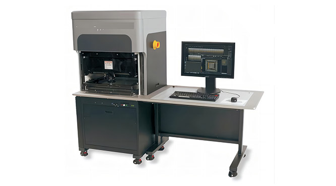
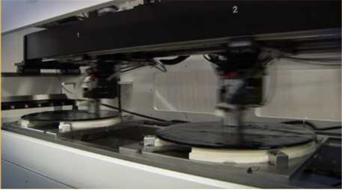
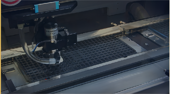


The latest automatic scannable on-line device for quality process management can scan lead frame bars, igbt power modules, multilayer ceramic chip capacitors, flip chips and other components
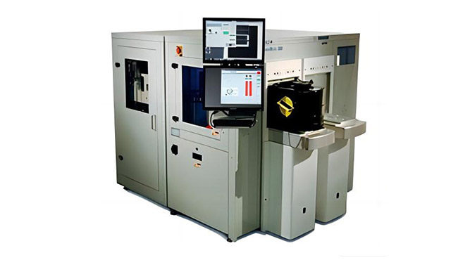
The W series is a fully automatic C-SAM system designed for wafer applications. Provides maximum sensitivity and high throughput for evaluating bonded wafer applications (SOI, MEMS, LED, 2.5D, and 3D)
■ D9650
■ AW300
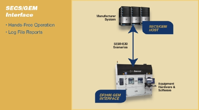
The latest automated scannable on-line device for quality process management, the DF2400 provides 2 to 7 times the throughput of conventional tools by scanning two trays simultaneously and using multiple probes
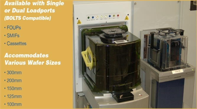
■ The device has automatic scanning of JEDEC trays or automatic box carrier parts
■ The Sonolytics software platform is an ideal solution for manufacturing field environments
The AW series features bonding between two wafers and a diameter of less than 5 microns that can detect stripping between thin wafers, called 200 Angstrom
AW features two or more scanning heads, staging stations, and drying stations designed to efficiently scan a second wafer while drying previously scanned wafers
Coming soon